Nanomaterials are those which have structured components with at least one dimension less than 100 nm. Materials that have one dimension in the nanoscale (and are extended in the other two dimensions) are layers, such as a thin films or surface coatings. Some of the features of computer chips come in this category. Materials, that are nanoscale in two dimensions (and extended in one dimension) include nanowires and nanotubes. Materials that are nanoscale in three dimensions are particles, for example, precipitates, colloids and quantum dots (tiny particles of semiconductor materials). Nanocrystalline materials, made up of nanometre-sized grains, also fall into this category. Some of these materials have been available for some time; others are genuinely new.
Two principal factors cause the properties of nanomaterials to differ significantly from other materials: increased relative surface area, and quantum effects. These factors can change or enhance properties such as reactivity, strength and electrical characteristics. As a particle decreases in size, a greater proportion of atom are found at the surface compared to those inside. For example, a particle of size 30 nm has 5% of its atoms on its surface, at 10 nm 20% of its atoms, and at 3 nm 50% of its atoms. Thus nanoparticles have a much greater surface area per unit mass compared with larger particles. As growth and catalytic chemical reactions occur at surfaces, this means that a given mass of material in nanoparticulate form will be much more reactive than the same mass of material made up of larger particles.
Significance of the Nanoscale
A nanometer (nm) is one thousand millionth of a meter. For comparison, a red blood cell is approximately 7,000 nm wide and a water molecule is almost 0.3nm across. People are interested in the nanoscale [which we define to be from 100nm down to the size of atoms (approximately 0.2nm)] because it is at this scale that the properties of materials can be very different from those at a larger scale. We define nanoscience as the study of phenomena and manipulation of materials at atomic, molecular and macromolecular scales, where properties differ significantly from those at a larger scale; and nanotechnologies as the design, characterization, production and application of structures, devices and systems by controlling shape and size at the nanometer scale. In some senses, nanoscience and nanotechnologies are not new. Chemists have been making polymers, which are large molecules made up of nanoscale subunits, for many decades and nanotechnologies have been used to create the tiny features on computer chips for the past 20 years. However, advances in the tools that now allow atoms and molecules to be examined and probed with great precision have enabled the expansion and development of nanoscience and nanotechnologies.
The bulk properties of materials often change dramatically with nano ingredients. Composites made from particles of nano-size ceramics or metals smaller than 100 nanometers can suddenly become much stronger than predicted by existing materials-science models. For example, metals with a so-called grain size of around 10 nanometers are as much as seven times harder and tougher than their ordinary counterparts with grain sizes in the hundreds of nanometers. The causes of these drastic changes stem from the weird world of quantum physics. The bulk properties of any material are merely the average of all the quantum forces affecting all the atoms. As you make things smaller and smaller, you eventually reach a point where the averaging no longer works.
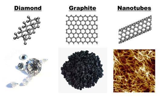
Type of nanomaterials on basis of Dimension
The properties of materials can be different at the nanoscale for two main reasons: First, nanomaterials have a relatively larger surface area when compared to the same mass of material produced in a larger form. This can make materials more chemically reactive (in some cases materials that are inert in their larger form are reactive when produced in their nanoscale form), and affect their strength or electrical properties. Second, quantum effects can begin to dominate the behaviour of matter at the nanoscale - particularly at the lower end - affecting the optical, electrical and magnetic behaviour of materials. Materials can be produced that are nanoscale in one dimension (for example, very thin surface coatings), in two dimensions (for example, nanowires and nanotubes) or in all three dimensions (for example, nanoparticles).
Nanoscale in one dimension
Thin films, layers and surfaces
One-dimensional nanomaterials, such as thin films and engineered surfaces, have been developed and used for decades in fields such as electronic device manufacture, chemistry and engineering. In the silicon integrated-circuit industry, for example, many devices rely on thin films for their operation, and control of film thicknesses approaching the atomic level is routine. Monolayers (layers that are one atom or molecule deep) are also routinely made and used in chemistry. Engineered surfaces with tailored properties such as large surface area or specific reactivity are used routinely in a range of applications such as in fuel cells and catalysts. The large surface area provided by nanoparticles, together with their ability to self assemble on a support surface, could be of use in all of these applications.
Nanoscale in two dimensions
Two dimensional nanomaterials such as tubes and wires have generated considerable interest among the scientific community in recent years. In particular, their novel electrical and mechanical properties are the subject of intense research.
a) Carbon nanotubes
Carbon nanotubes (CNTs) are typically a few nanometres in diameter and several micrometres to centimetres long (Fig.2). CNTs have assumed an important role in the context of nanomaterials, because of their novel chemical and physical properties.
 |
| Fig. 2 |
They are mechanically very strong, flexible, and can conduct electricity extremely well. All of these remarkable properties give CNTs a range of potential applications: for example, in reinforced composites, sensors, nanoelectronics and display devices.
b) Inorganic nanotubes
Inorganic nanotubes and inorganic fullerene-like materials based on layered compounds have excellent lubricating properties, resistance to shockwave
c) Nanowires
Nanowires are ultrafine wires or linear arrays of dots, formed by self-assembly. They can be made from a wide range of materials. Semiconductor nanowires made of silicon (Fig 3), gallium nitride and indium phosphides have demonstrated remarkable optical, electronic and magnetic characteristics.
| Fig 3 Silicon nanowire |
Nanowires have potential applications in high-density data storage; either as magnetic read heads or as patterned storage media.
d) Biopolymers
The variability and site recognition of biopolymers, such as DNA molecules, offer a wide range of opportunities for the self-organization of wire nanostructures into much more complex patterns eg. Biocompatible sensors and small, simple motors. Such self-assembly of organic backbone nanostructures is often controlled by weak interactions, such as hydrogen bonds, hydrophobic, or van der Waals interactions. The combination of one-dimensional nanostructures consisting of biopolymers and inorganic compounds opens up a number of scientific and technological opportunities.
Nanoscale in three dimensions
a) Nanoparticles
Nanoparticles are often defined as particles of less than 100nm in diameter. Nanoparticles are of interest because of the new properties (such as chemical reactivity and optical behaviour) that they exhibit, compared with larger particles of the same materials. For example, titanium dioxide (Fig. 4) and zinc oxide become transparent at the nanoscale, however are able to absorb and reflect UV light, and have found application in sunscreens.
 |
| Fig. 4 Titanium oxides |
Nanoparticles have a range of potential applications: in the short-term in new cosmetics, textiles and paints; in the longer term, in methods of targeted drug delivery where they could be to used deliver drugs to a specific site in the body. Nanoparticles can also be arranged into layers on surfaces, providing a large surface area and hence enhanced activity, relevant to a range of potential applications such as catalysts.
b) Fullerenes (carbon 60)
C60 are spherical molecules about 1nm in diameter, comprising 60 carbon atoms arranged as 20 hexagons and 12 pentagons: the configuration of a football (Fig 5).
| Fig 5 Buckminster Fullerene C60 |
Several applications are envisaged for fullerenes, such as miniature ‘ball bearings’ to lubricate surfaces, drug delivery machines and in electronic circuits.
c) Dendrimers
| Fig. 6 |
Dendrimers (Fig 6) are spherical polymeric molecules, formed through a nanoscale hierarchical self-assembly process. They are used in conventional applications such as coatings and inks; they can act as nanoscale carrier molecules and as such could be used in drug delivery. Environmental clean-up could be assisted by dendrimers as they can trap metal ions, which could then be filtered out of water with ultra-filtration techniques.
d) Quantum dots
If semiconductor particles are made small enough (Fig. 7), quantum effects come into play, which limit the energies at which electrons and holes (the absence of an electron) can exist in the particles. As energy is related to wavelength (or colour), this means that the optical properties of the particle can be finely tuned depending on its size.
| Fig. 7 |
Thus, particles can be made to emit or absorb specific wavelengths (colours) of light, merely by controlling their size. Recently, quantum dots have found applications in composites, solar cells and fluorescent biological labels (for example to trace a biological molecule) which use both the small particle size and tuneable energy levels. Recent advances in chemistry have resulted in the preparation of monolayer-protected, high-quality, monodispersed, crystalline quantum dots as small as 2 nm in diameter, which can be conveniently treated and processed as a typical chemical reagent.